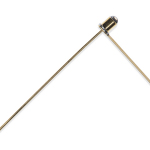
KP-M Achieves Higher Quality through Inspection Process at Higher Temperature.
TOKYO–(BUSINESS WIRE)–Kyoto Semiconductor Co., Ltd. (President and CEO Tsuneo Takahashi, Head office: Fushimi-ku, Kyoto city), a leading optical device solution manufacturer with world-class technologies and Japanese quality, has announced the new KP-M monitor photodiode, KPDE008LS-A-RA-HQ.
KP-M monitor photodiodes are used to monitor the laser output of optical communication equipment.
Higher quality devices are required as the expansion of digital transformation and 5G communications progresses. The “KPDE008LS-A-RA-HQ” has achieved higher quality by adding the probing process at higher temperature.
- A new wafer prober*1 has been introduced to inspect the electrical characteristics of semiconductor wafers while heated to high temperatures. This allows the inspection to test the temperature (T=75℃) close to the absolute maximum rated value of the operating temperature of the product. Since the full inspection is implemented to wafers with this prober, higher quality products under higher temperatures can be realized.
- Then the sample inspection is conducted by wafer and the sampled products are sent to the burn-in test. The samples are heated up to the high temperature of 175℃ and their performance are inspected. If any of the sample products does not meet the standard, all the products on the same wafer are not shipped. This screening by wafer enables us to offer higher quality products.
Mass production of the KP-M monitor photodiode “KPDE008LS-A-RA-HQ” is scheduled to start on December 1, 2021.
For more information
https://www.kyosemi.co.jp/en/products/kpde008ls-a-ra-hq/
*1 Wafer prober: A device that inspects the electrical characteristics of semiconductor wafers. The electrical characteristics of the semiconductor wafer are measured by bringing the probe needle into contact with the individual electrodes formed on the wafer.
About Kyoto Semiconductor
Kyoto Semiconductor was established in 1980 in Kyoto as a dedicated manufacturer of optical semiconductors. The semiconductors manufactured offer superlative performance and precision, suited for use in optical transmission. They are manufactured end-to-end, including pre- and post-processing, and together with Kyoto Semiconductor’s unique packaging technology, at our location in Japan and made available to customers around the world. Kyoto Semiconductor leads the industry with world-standard technologies for optical device solutions based on Japanese quality and attention to production detail.
Company Website: https://www.kyosemi.co.jp/
*Product names, company names, and organization names mentioned in this press release are trademarks or registered trademarks of their respective companies.
*All contents of this press release are as of the date of publication and are subject to change without notice.
Contacts
Media Relations, Kyoto Semiconductor Co., Ltd.
Naoko Kodama
Email: [email protected]
If you enjoyed this article and want to receive more valuable industry content like this, click here to sign up for our digital newsletters!


